Design for Test in PCB Electronics: DFT Strategies That Prevent Manufacturing Blind Spots
Design for Test, often called DFT or design for testability, means designing a PCB so it can be inspected, probed, programmed, debugged, and verified during manufacturing without unnecessary rework. A circuit can look correct in CAD and still become expensive to manufacture if the assembler cannot access critical nets, verify hidden solder joints, isolate faults, or run repeatable functional tests.
For OEMs, DFT is not only an engineering detail. It affects yield, troubleshooting time, documentation, field reliability, and how smoothly a product moves from prototype to production.
At ANZER USA, I look at DFT as part of the same discipline as DFM and DFA. If the board cannot be built, inspected, tested, and documented in a controlled way, the design is not ready for production.
What Design for Test Means in PCB Assembly
Design for Test is the practice of building test access into the PCB design before the layout is released for fabrication and assembly.
A good DFT plan answers practical manufacturing questions:
- Can critical nets be accessed by ICT, flying probe, or boundary scan?
- Can power rails, grounds, clocks, resets, regulators, and communication lines be verified?
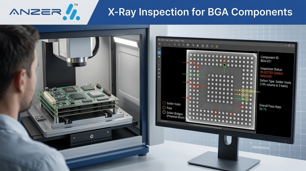
- Can hidden solder joints under BGAs, QFNs, LGAs, or fine-pitch devices be inspected?
- Can firmware be loaded or verified without manual workaround?
- Can the contract manufacturer isolate a fault quickly when a board fails?
- Can the same test process be repeated across prototype, pre-production, and production builds?
DFT does not replace good schematic design, layout discipline, IPC workmanship standards, AOI, X-ray, or functional testing. It connects those pieces into a usable manufacturing test strategy.
Why DFT Should Start Before PCB Layout Is Locked
The most expensive time to add testability is after the board is already routed.
At that stage, the layout may be crowded, mechanical keep-outs may already be fixed, and test points may compete with high-speed routing, thermal areas, connectors, shielding, or enclosure constraints. That is why DFT should be discussed during schematic review and early layout, not after the Gerbers are complete.
A practical DFT review should happen before these decisions are frozen:
| Design Area | DFT Question to Ask | Risk If Ignored |
|---|---|---|
| Test points | Are critical nets accessible from the preferred test side? | Manual probing, low coverage, slow troubleshooting |
| Power rails | Can each voltage rail be verified safely? | Shorts, regulator faults, or voltage issues missed until system test |
| Programming | Is there controlled access for firmware loading or verification? | Manual handling, inconsistent programming, delayed bring-up |
| Boundary scan | Are JTAG-capable devices connected and documented correctly? | Reduced visibility into dense digital interconnects |
| Hidden joints | Are BGA/QFN areas inspectable by X-ray where needed? | Hidden solder defects missed by visual inspection |
| Functional test | Are test modes, connectors, loads, and expected outputs defined? | Ambiguous pass/fail criteria |
| Documentation | Are test procedures, drawings, BOM, and revision controls complete? | Slower quoting, delays, poor traceability |
This is where custom electronic design services and electronic design for manufacturability should connect. DFT is not a separate afterthought. It belongs inside the design-for-manufacturing conversation.
Core DFT Strategies for PCB Electronics
Plan the test strategy before layout release
Start with the production expectation. A prototype board, a low-volume industrial controller, and a regulated medical or aerospace assembly may need different test approaches.
Before layout release, define:
- Expected build volume
- Product risk level
- Required documentation
- Critical circuits
- Required inspection methods
- Functional test needs
- Firmware programming requirements
- Test coverage expectation
- Prototype-to-production path
A prototype may use flying probe and functional testing. A production assembly may justify ICT fixtures. A dense digital board may need boundary scan. A high-reliability assembly may require a hybrid strategy using AOI, X-ray, ICT or flying probe, functional testing, and burn-in where appropriate.
Add accessible test points for critical nets
Test points allow production test equipment to contact the circuit electrically. They are especially important for power, ground, regulators, reset lines, clock circuits, communication interfaces, programming lines, and analog reference points.
Not every product needs the same level of access, but every product needs a clear test philosophy.
Good test-point planning should consider:
- Probe access from the preferred side of the board
- Mechanical clearance around components
- Fixture access and board support
- Power and ground distribution
- High-speed signal impact
- Conformal coating or potting requirements
- Whether the product will move from prototype to higher-volume production later
For a deeper implementation guide, use ANZER’s supporting article on Design for Testing PCB test point placement for ICT.
Use boundary scan where physical access is limited
Boundary scan, often associated with JTAG, is useful when dense components, BGAs, or high-pin-count digital devices make physical probing difficult. IEEE 1149.1 provides a standardized test access port and boundary-scan architecture for testing interconnections between integrated circuits after assembly.
Boundary scan can help verify digital interconnects that are difficult to reach with physical probes. It can also support programming, debug, and board bring-up when designed correctly.
For boundary scan to work well, the design team should document:
- JTAG chain order
- TDI/TDO routing
- Device support files
- Pull-ups, resets, and boot modes
- Access connector or test pad strategy
- Voltage domains
- Expected test coverage
Boundary scan is not a full replacement for ICT, AOI, X-ray, or functional test. It is one tool in the DFT plan.
Choose the right production test method
The correct test method depends on design complexity, volume, board density, risk, and production economics.
| Test Method | Best Fit | What It Helps Detect | DFT Requirement |
|---|---|---|---|
| AOI | SMT assemblies and visual solder/component checks | Missing parts, polarity, placement, visible solder defects | Clear component visibility and inspection-friendly layout |
| X-ray inspection | BGAs, QFNs, hidden solder joints, dense assemblies | Voids, bridges, opens, hidden solder defects | Layout and package selection that supports meaningful inspection |
| Flying probe | Prototypes, low-volume builds, early engineering runs | Opens, shorts, component values, basic electrical faults | Accessible pads or probeable nodes |
| ICT / bed-of-nails | Repeat production, higher-volume assemblies | Shorts, opens, wrong values, component-level faults | Planned test points and fixture access |
| Boundary scan | Dense digital boards and limited physical access | Digital interconnect faults and certain device-level test conditions | JTAG-capable devices and documented chain |
| Functional testing | Product-level behavior verification | Whether the board performs the intended function | Defined test procedure, fixtures, loads, and pass/fail criteria |
| Burn-in testing | High-reliability or stress-screened products | Early-life failures under electrical/thermal stress | Defined stress conditions and acceptance criteria |
ANZER supports in-house AOI, X-ray inspection, ICT, flying probe testing, functional testing, and burn-in testing where specified for the build.
Design for inspection, not only electrical test
DFT is often discussed around electrical testing, but inspection access matters too.
If components are too close together, hidden under shielding, placed near tall mechanical features, or buried under coating without a test plan, inspection becomes harder. That can create avoidable risk during manufacturing.
Good inspection-aware design considers:
- Component orientation consistency
- Polarity marking visibility
- Fiducial placement
- BGA/QFN inspection needs
- Connector access
- Labeling and serialization space
- Coating keep-out areas
- Test access after mechanical integration
This is especially important when the PCBA becomes part of a larger box build assembly or includes wire harness and cable assembly routing.
DFT for Aerospace, Medical, and Industrial Electronics
High-reliability electronics require more disciplined test planning than basic commercial assemblies.
For aerospace, medical, industrial automation, and other reliability-sensitive products, DFT should support:
- Traceability from component to finished assembly
- Documented test procedures
- IPC workmanship expectations
- Controlled inspection steps
- Clear pass/fail limits
- Revision-controlled drawings and test records
- Functional verification under realistic operating conditions
- Risk-based testing for critical circuits
ANZER’s certifications and quality systems support regulated-industry work, including ISO 9001:2015, ISO 13485:2016, AS9100D, IPC-A-610 workmanship discipline, and Class 2/Class 3 assembly capability where applicable.
For buyers comparing suppliers, certifications alone are not enough. Ask how the contract manufacturer handles DFT review, test coverage, documentation, inspection, traceability, and failure feedback.
What to Include in a DFT-Ready RFQ Package
A PCB assembly quote is more accurate when the EMS partner can see the test requirements early.
Include these items when requesting a DFT review or PCB assembly quote:
- Schematic
- PCB layout files
- Gerber or ODB++/IPC-2581 output where available
- Bill of Materials
- Assembly drawing
- Fabrication drawing
- Critical net list
- Functional test requirements
- Firmware programming requirements
- Known high-risk components
- BGA/QFN package notes
- Connector and harness requirements
- Enclosure or box build constraints
- Regulatory or customer quality requirements
- Expected prototype, pilot, and production volumes
If the design is still in progress, share it before final release. A DFT issue found during layout review is usually easier to fix than one found after boards are already fabricated.
Common DFT Mistakes That Create Manufacturing Risk
Waiting until after layout completion
If test access is added late, it may conflict with routing, component placement, shielding, or mechanical packaging.
Assuming functional test is enough
Functional testing tells you whether the product works under defined conditions. It may not isolate component-level faults efficiently. ICT, flying probe, AOI, X-ray, and boundary scan can find different defect types.
Ignoring programming access
Firmware loading and verification should be planned. Relying on temporary soldered wires or manual workarounds creates variation and slows production.
Making critical nets inaccessible
Power rails, reset lines, clocks, communication buses, and analog references should not be impossible to probe or verify.
Forgetting test after coating, potting, or box build
If the assembly will be coated, potted, enclosed, or integrated into a system, the test sequence must be planned before those steps happen.
Treating prototype test strategy as production strategy
A prototype can often be manually debugged. Production needs repeatability, documentation, and efficient fault isolation.
How ANZER Supports DFT From Prototype to Production
ANZER USA supports OEMs with design, DFM/DFA review, BOM optimization, PCB fabrication, SMT and through-hole assembly, inspection, testing, coating, potting, wire harness assembly, box build integration, and production support from our Akron, Ohio facility.
For DFT specifically, ANZER can help buyers review:
- Test point strategy
- ICT vs flying probe fit
- Boundary-scan opportunities
- AOI and X-ray inspection needs
- Functional test planning
- Burn-in requirements where applicable
- Documentation needed for traceability
- Prototype-to-production transition risks
This matters most when the product is not a simple one-time prototype. If the board may move into pilot or production, the test strategy should be built into the design before the first release.
ANZER’s no-MOQ model and dedicated prototype production line also help engineering teams test early without changing suppliers when the product moves toward production.
Conclusion
Design for Test is one of the most practical ways to reduce manufacturing uncertainty in PCB electronics. It gives the assembler access to the right nets, supports faster fault isolation, improves inspection planning, and creates a stronger bridge between engineering design and production reality.
The best time to solve testability problems is before the PCB is released.
If your team is preparing a new PCB design, prototype build, or production transfer, ANZER USA can review the design for manufacturability, assembly, test access, inspection risk, and production readiness before the build begins.
CTA: Send your schematic, BOM, assembly drawing, and expected build requirements to ANZER for a practical PCB assembly and DFT review.
FAQs
What is Design for Test in PCB electronics?
Design for Test is the practice of designing a PCB so it can be inspected, probed, programmed, debugged, and verified during manufacturing. It helps the assembler detect faults such as shorts, opens, wrong component values, missing parts, hidden solder issues, and functional failures.
Is DFT the same as DFM?
No. DFM focuses on whether the board can be manufactured efficiently and reliably. DFT focuses on whether the finished assembly can be tested efficiently and repeatably. In a strong PCB assembly process, DFM and DFT should be reviewed together.
Do all PCBs need test points?
Most PCB assemblies benefit from some level of test access, especially on power rails, ground, reset, clock, programming, and critical signal nets. The number and placement of test points depends on product risk, board density, expected volume, and test method.
When should I use ICT instead of flying probe?
Flying probe is often a better fit for prototypes, engineering builds, and low-volume production because it avoids custom fixture cost. ICT is typically stronger for repeat production where fixture investment can support faster, repeatable testing. The decision should be made during DFT review.
Does boundary scan replace physical test points?
No. Boundary scan can reduce the need for some physical probing on compatible digital devices, but it does not replace all inspection, ICT, flying probe, X-ray, or functional testing. It works best as part of a hybrid test strategy.
To learn more about PCB Assembly, read our WHITEPAPER!