
Design for Test in PCB Electronics: DFT Strategies That Prevent Manufacturing Blind Spots
Design for Test, often called DFT or design for testability, means designing a PCB so it can be inspected, probed, programmed, debugged, and verified during manufacturing without unnecessary rework. A circuit can look correct in CAD and still become expensive to manufacture if the assembler…

PCB Assembly: Controlling Moisture in Semiconductor Devices
Controlling moisture in semiconductor devices during PCB (Printed Circuit Board) assembly is crucial for several reasons: Manufacturers often use techniques such as vacuum-sealed packaging, humidity-controlled storage, and careful handling procedures in controlling moisture in semiconductor devices during PCB assembly. These measures help ensure that the…

PCB Assembly: Monitoring Quality and Process Performance
Monitoring product quality and process performance in PCB (Printed Circuit Board) assembly ensures that the final electronic products meet the desired standards and specifications. Here’s a step-by-step guide on how to effectively monitor quality and process performance in PCB assembly: By following these steps and…

Corrective Action in PCB Assembly: A Practical 8-Step Process
Corrective action in PCB assembly is the documented process used to eliminate the cause of a confirmed nonconformance and prevent it from recurring. It is not the same as sorting, reworking, repairing, or replacing affected boards. Those activities correct the product. A complete corrective action…
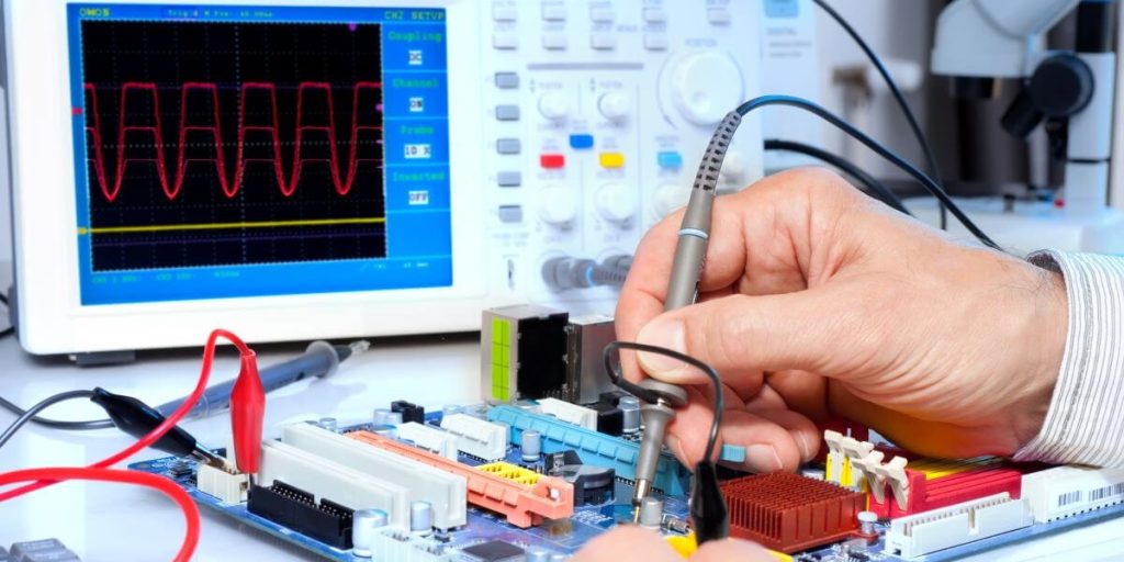
Electronic Assembly Root Cause Analysis: How OEMs Find and Prevent PCB Assembly Defects
Electronic assembly root cause analysis is the process of finding the real reason a PCB assembly defect happened, not just repairing the visible symptom. For OEMs, that matters because a solder bridge, intermittent connection, component shift, or functional test failure can point to deeper issues…