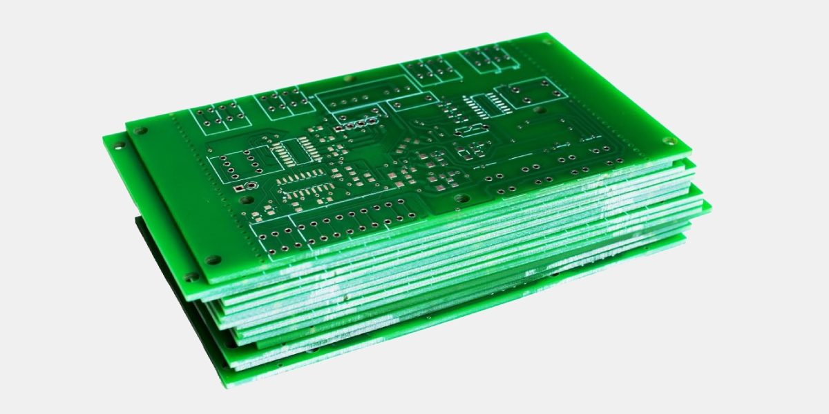
Bare PCB Manufacturing Process: 16 Steps | ANZER
A bare PCB is manufactured by converting approved design data into a physical, unpopulated circuit board. The process typically includes design-for-manufacturability review, layer imaging and etching, multilayer lamination, drilling, hole-wall plating, outer-layer processing, solder mask, surface finishing, profiling, electrical testing, and final inspection.
The exact sequence depends on whether the board is single-sided, double-sided, multilayer, rigid, flex, or rigid-flex. However, the purpose remains the same: produce a board whose physical structure and electrical connections match the approved fabrication requirements before any components are installed.
What Is a Bare PCB?
A bare printed circuit board is a fabricated circuit board that has not yet been populated with electronic components.
A completed bare PCB may already contain:
- Copper traces and planes
- Pads for component attachment
- Plated through-holes and vias
- Solder mask
- Silkscreen or legend markings
- Edge connectors
- A protective surface finish
- Routed edges, slots, cutouts, and mounting holes
It does not contain installed resistors, capacitors, integrated circuits, connectors, or other electronic components.
That distinction matters when requesting quotes. PCB fabrication creates the physical board. PCB assembly installs and solders the components onto it.
For a broader explanation of board structure and terminology, see ANZER’s guide to printed circuit boards and their functions.
Bare PCB vs. PCBA
| Requirement | Bare PCB fabrication | PCB assembly |
|---|---|---|
| Primary output | Unpopulated circuit board | Populated and soldered circuit board |
| Main inputs | Fabrication data, drill files, stack-up, drawing, netlist | BOM, centroid data, assembly drawings, approved bare boards |
| Main processes | Imaging, etching, lamination, drilling, plating, solder mask, finishing | Solder paste printing, component placement, reflow, through-hole insertion, soldering |
| Common inspection focus | Copper geometry, hole plating, registration, dimensions, electrical continuity | Component placement, polarity, solder joints, workmanship, functionality |
| Common terminology | PCB, printed board, bare board | PCBA, printed circuit board assembly |
A project may use one supplier for fabrication and another for assembly. It may also use an integrated manufacturing partner that can review the design, fabricate the board, assemble the components, test the PCBA, and support the transition into production.
The Bare PCB Manufacturing Process
1. Review the fabrication data
Manufacturing begins with a controlled set of digital files and fabrication instructions.
Depending on the project and supplier, the package may use:
- Gerber RS-274X files
- ODB++ data
- IPC-2581 data
- NC drill files
- Routing data
- Fabrication drawings
- Layer stack-up information
- Material and copper specifications
- Controlled-impedance requirements
- Netlist data
Each copper layer, solder mask layer, legend layer, drill feature, and board outline must be clearly defined.
A bill of materials is not normally needed to manufacture only the bare board. The BOM becomes necessary when components will be procured and assembled.
For more detail on the most widely recognized fabrication format, review ANZER’s explanation of Gerber files for PCB manufacturing.
2. Perform DFM and CAM review
Before production, manufacturing engineers review the data for completeness and manufacturability.
Typical checks include:
- Layer count and sequence
- Trace widths and spacing
- Annular-ring dimensions
- Finished and drilled hole sizes
- Hole-to-copper clearances
- Copper-to-board-edge clearances
- Solder mask openings
- Via structure and aspect ratio
- Controlled-impedance information
- Copper distribution and balance
- Board outline, slots, and cutouts
- Panelization and tooling requirements
- Conflicts between the drawing and electronic data
The approved data is then processed using computer-aided manufacturing, or CAM, software. CAM preparation creates the imaging, drilling, routing, inspection, and electrical-test data used throughout fabrication.
Resolving these questions before production is substantially less disruptive than finding them after imaging, drilling, or lamination has begun. ANZER supports this stage through PCB design-for-manufacturability review and a practical PCB DFM checklist.
3. Select and prepare the PCB material
The fabricator selects the laminate, copper foil, prepreg, and other materials specified by the design.
Material selection affects:
- Electrical performance
- Thermal behavior
- Mechanical strength
- Dimensional stability
- Flammability requirements
- Moisture behavior
- Assembly temperature exposure
- Long-term reliability
FR-4 is commonly used for rigid printed circuit boards, but the correct material must be selected from the product’s actual electrical, thermal, environmental, and regulatory requirements.
For multilayer boards, the selected cores and prepreg must also match the approved stack-up.
4. Image the inner copper layers
For a multilayer PCB, the internal copper layers are processed before lamination.
A photo-sensitive resist is applied to the copper-clad core. The required circuit pattern is transferred to the resist using an imaging process, commonly laser direct imaging or another controlled photolithographic method.
The exposed and developed resist protects the copper that must remain as circuitry.
5. Etch the inner layers
The unwanted copper is chemically removed from each imaged inner layer.
After etching, the remaining copper forms the required internal traces, pads, power planes, and ground planes.
The resist is then stripped away, and the processed layer is cleaned for inspection.
Etching control is important because excessive or insufficient etching can alter conductor geometry. This can affect current capacity, impedance, spacing, and overall conformity to the design.
6. Inspect the inner layers
Inner layers are inspected before they are permanently laminated into the board.
Automated optical inspection can compare the manufactured copper pattern against the design data and identify conditions such as:
- Opens
- Shorts
- Missing copper
- Excess copper
- Incorrect feature geometry
- Registration errors
This inspection must occur before lamination because the internal circuitry becomes difficult to access once the layers are bonded together.
7. Build and laminate the multilayer stack
The inspected inner layers are arranged with sheets of prepreg and external copper foil according to the approved stack-up.
The complete layup is bonded under controlled heat and pressure. The prepreg resin flows and cures, forming one mechanically integrated multilayer panel.
Lamination parameters must be appropriate for the selected materials, board thickness, copper distribution, and stack-up. Poor control can contribute to layer misregistration, voids, delamination, bow, twist, or inconsistent finished thickness.
Single-sided and some double-sided boards do not require the same multilayer lamination sequence.
8. Drill holes, vias, and mechanical features
Computer-controlled drilling equipment creates the holes required for:
- Component leads
- Plated through-holes
- Vias
- Mounting hardware
- Tooling
- Mechanical alignment
- Board attachment
The drill program must correspond with the fabrication drawing and electronic data.
Different designs may contain through vias, blind vias, buried vias, or microvias. Each via structure requires compatible materials, drilling methods, plating processes, and inspection requirements.
9. Clean and prepare the drilled holes
Mechanical drilling can leave resin and debris on the hole walls. The panel is therefore cleaned and desmeared before conductive plating.
This preparation exposes clean material surfaces and helps the deposited copper adhere correctly inside the holes.
Hole preparation is a significant reliability step. Inadequate cleaning or weak plating can compromise electrical connections between PCB layers.
10. Deposit and plate copper
A thin conductive copper layer is first deposited onto the nonconductive hole walls. Additional electrolytic copper is then plated to build the required conductor thickness.
This process creates electrical connections between the copper layers and forms plated through-holes and vias.
Plating requirements should be defined by the applicable drawing, procurement specification, and product performance requirements.
For rigid boards, IPC-6012F addresses qualification and performance requirements for several rigid printed-board constructions. The exact standard, revision, class, amendments, and customer requirements should be stated in the contract documentation rather than assumed.
11. Form the outer-layer circuitry
The outer copper layers are coated with resist and imaged with the external circuit pattern.
The exposed conductive features are plated as required, and the unwanted outer-layer copper is etched away. After the resist and temporary plating materials are removed, the finished traces, pads, and external copper features remain.
At this stage, the physical electrical network of the board has been formed.
12. Apply solder mask
Solder mask is applied over the board and selectively opened where exposed copper is required for soldering, testing, connectors, or other functions.
Solder mask helps:
- Protect copper from contamination and handling
- Reduce unintended solder bridging
- Define component pads
- Improve insulation between adjacent features
- Support the later assembly process
Mask registration and opening dimensions must be compatible with the pad geometry and component technology.
13. Add legend or silkscreen markings
The legend identifies information that may be needed during assembly, inspection, servicing, or field use.
Markings can include:
- Reference designators
- Polarity indicators
- Connector labels
- Test-point identifiers
- Part numbers
- Revision information
- Warning symbols
- Manufacturer identification
Legend markings should remain clear of solderable surfaces unless the drawing specifically permits otherwise.
14. Apply the surface finish
A surface finish protects exposed copper and creates an appropriate interface for soldering, wire bonding, connectors, or other attachment processes.
Common options include:
| Surface finish | Common selection considerations |
|---|---|
| HASL | Established solderable finish; surface flatness should be evaluated for fine-pitch parts |
| ENIG | Flat surface suited to many fine-pitch and BGA applications; requires controlled processing |
| OSP | Flat, lead-free coating with specific handling, storage, and thermal-cycle considerations |
| Hard gold or gold fingers | Used where connector contact surfaces require wear resistance |
| Selective finishes | Used when different board areas require different surface properties |
The correct finish depends on component pitch, solder alloy, storage conditions, assembly process, contact wear, environmental exposure, thermal cycles, and product reliability requirements.
ANZER’s verified PCB fabrication capabilities include multiple surface-finish options, including ENIG, HASL, OSP, gold fingers, and other application-specific finishes.
15. Route, score, and separate the boards
The fabricated panel is profiled into the required board shape.
Depending on the design and assembly plan, separation features may include:
- CNC-routed outlines
- V-scores
- Breakaway tabs
- Mouse-bite perforations
- Internal cutouts
- Slots
- Beveled connector edges
Panelization should consider material use, board support during assembly, component clearance, depanelization stress, fiducial placement, tooling, and downstream handling.
16. Complete electrical testing and final inspection
Before release, the bare PCB is tested and inspected against the approved requirements.
Quality activities may include:
- Electrical continuity testing
- Isolation or short-circuit testing
- Automated optical inspection
- Dimensional verification
- Hole and slot measurement
- Solder mask inspection
- Surface-finish inspection
- Bow and twist evaluation
- Visual inspection
- Controlled-impedance testing, when specified
- Coupon or microsection evaluation, when specified
- Verification of markings and traceability
IPC-A-600M provides visual acceptability guidance for printed boards. It should be used together with the applicable performance specification, procurement documentation, fabrication drawing, and customer requirements.
IPC-A-610 should not be treated as the primary bare-board acceptance standard. IPC-A-610 addresses electronic assembly acceptability after components have been installed. Bare-board and assembled-board quality requirements are related, but they are not interchangeable.
What Determines PCB Fabrication Complexity?
The number of manufacturing operations alone does not determine whether a board is easy or difficult to produce.
The following requirements can significantly affect process control, cost, production planning, and supplier fit:
- Higher layer count
- Very thin or very thick construction
- Tight trace and spacing requirements
- Small drilled holes
- High via aspect ratios
- Blind, buried, or stacked vias
- Controlled impedance
- Fine-pitch component pads
- Via-in-pad construction
- Rigid-flex transitions
- Specialty laminate materials
- Heavy copper
- Tight dimensional tolerances
- Multiple surface finishes
- Edge plating
- Special testing or documentation
- High-reliability acceptance requirements
A board that looks simple on the schematic can still be difficult to fabricate. The stack-up, hole structure, copper geometry, tolerances, materials, and inspection requirements must be evaluated together.
How Bare PCB Quality Affects Assembly
Bare-board fabrication quality directly influences later SMT and through-hole assembly.
Examples include:
- Misregistered solder mask can expose or obstruct pads.
- Uneven surface finish can affect solder-paste printing and fine-pitch placement.
- Board bow or twist can interfere with stencil contact, component placement, and reflow.
- Weak hole-wall plating can create intermittent or open layer connections.
- Incorrect pad geometry can increase soldering defects.
- Contaminated or oxidized surfaces can reduce solderability.
- Dimensional errors can prevent the PCB from fitting its enclosure or mating hardware.
- Incorrect stack-up construction can affect impedance and signal behavior.
This is why fabrication, assembly, and test requirements should be considered during design rather than treated as separate decisions.
ANZER can support a project from custom electronic design and layout through PCB fabrication, SMT and through-hole production, testing, coating, potting, wire harnesses, and box-build integration.
What to Include in a Bare PCB RFQ
A complete RFQ produces a more accurate technical review than sending only copper-layer files.
Include the following where applicable:
Design and fabrication files
- Gerber, ODB++, or IPC-2581 data
- NC drill files
- Rout or profile data
- Netlist
- Fabrication drawing
- Panel drawing, when customer-controlled
Construction requirements
- Board type
- Layer count
- Finished board thickness
- Approved stack-up
- Laminate or material requirements
- Copper weight
- Finished hole sizes
- Via structures
- Controlled-impedance requirements
- Surface finish
- Solder mask and legend requirements
Mechanical requirements
- Overall dimensions
- Slots and cutouts
- Edge tolerances
- Connector bevels
- Scoring or routing requirements
- Panelization constraints
Quality and commercial requirements
- Prototype or production status
- Order quantity
- Required standards and revisions
- Acceptance class
- Inspection and testing requirements
- Documentation and traceability needs
- Regulatory or customer-specific requirements
- Target production schedule
- Packaging requirements
Do not rely on default assumptions for safety-critical, regulated, controlled-impedance, or high-reliability products. Put the requirements in the drawing, purchase order, specification, or approved quality documentation.
How to Evaluate a Bare PCB Manufacturer
Do not compare fabricators on unit price alone. Evaluate whether the supplier can consistently produce the required construction and support the later assembly process.
Ask:
- Can the supplier manufacture the required board type, materials, stack-up, vias, tolerances, and finish?
- Does the supplier perform a documented DFM and CAM review?
- How are drawing conflicts or incomplete files resolved?
- What electrical testing is included?
- Which IPC specifications and acceptance criteria can be supported?
- How are materials, process revisions, and production lots traced?
- Can the same partner support assembly and product-level testing?
- How will prototype changes be transferred into production?
- Which inspection records or certificates are available?
- What information is needed before a reliable quote can be issued?
The right manufacturing route depends on the product. A prototype, regulated medical assembly, aerospace control, industrial controller, and high-volume commercial board may require different process controls and documentation.
ANZER PCB Manufacturing Support
ANZER provides PCB fabrication and electronic manufacturing support from Akron, Ohio.
Verified capabilities include:
- FR-4 printed circuit boards
- Multilayer PCBs
- Rigid PCBs
- Flex PCBs
- Rigid-flex PCBs
- PCB layout and design support
- DFM and DFA review
- Multiple surface-finish options
- Prototype and production support
- SMT, through-hole, and mixed-technology assembly
- AOI, X-ray, ICT, flying-probe, functional, and burn-in testing
- In-house conformal coating and potting
- Wire harness and cable assembly
- Box-build integration
ANZER operates under ISO 9001:2015, ISO 13485:2016, and AS9100D quality management systems. Assembly programs can also be managed to IPC Class 2 or Class 3 workmanship requirements when specified.
The objective is not simply to produce a bare board. It is to create a manufacturable foundation that can move into assembly, inspection, testing, and production without avoidable technical surprises.
For projects moving beyond the first fabrication run, review how to manage the transition from PCB prototype to production.
FAQs
What is a bare PCB?
A bare PCB is a fabricated printed circuit board with copper circuitry, drilled and plated holes, solder mask, legend markings, and a specified surface finish, but no electronic components have been installed.
What is the difference between PCB fabrication and PCB assembly?
PCB fabrication creates the unpopulated circuit board. PCB assembly, or PCBA, installs and solders electronic components onto the fabricated board using SMT, through-hole, or mixed-technology processes.
What files are required to manufacture a bare PCB?
A complete fabrication package commonly includes Gerber, ODB++, or IPC-2581 design data, NC drill and route files, a fabrication drawing, stack-up requirements, material and copper specifications, controlled-impedance requirements when applicable, and a netlist for electrical verification.
How are bare PCBs tested?
Testing may include automated optical inspection, electrical continuity and isolation testing, dimensional checks, visual inspection, and additional coupon, impedance, microsection, or acceptance testing when specified by the drawing, purchase order, or applicable standard.
Which PCB surface finish should be selected?
The correct surface finish depends on component pitch, soldering process, storage and handling needs, environmental requirements, connector wear, cost, and the number of expected thermal cycles. ENIG, HASL, OSP, and hard-gold finishes serve different applications and should be selected during design and DFM review.
Request a PCB Manufacturing Review
A dependable fabrication quote starts with complete design data and clearly defined quality requirements.
Send ANZER your fabrication files, drawing, stack-up, material requirements, quantities, testing requirements, and intended application. The team can review the package for manufacturability and determine the appropriate route from bare PCB fabrication through assembly and product integration.


