Functional Testing vs ICT vs AOI vs X-ray: What PCB Assembly Buyers Need to Know
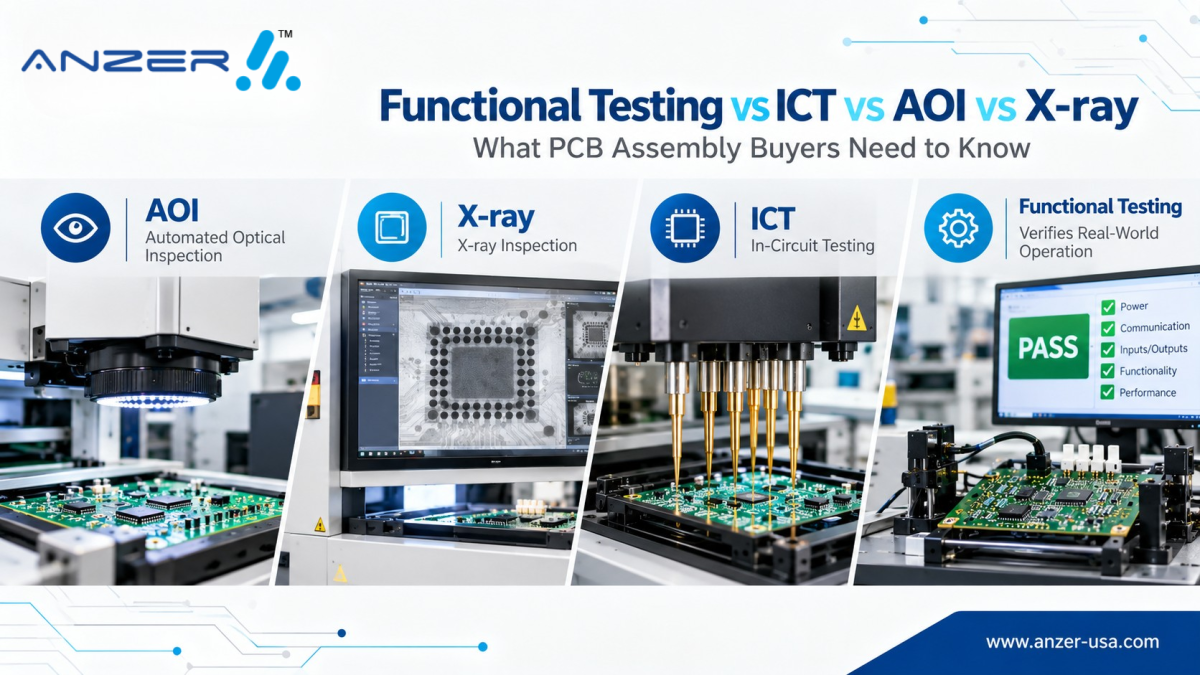
When an OEM evaluates PCB assembly testing, four terms appear repeatedly: AOI, X-ray inspection, ICT, and functional testing. They are not interchangeable.
AOI primarily inspects visible assembly conditions. X-ray inspection helps reveal hidden solder connections. ICT evaluates electrical characteristics. Functional testing checks whether the assembled electronics actually operate as intended.
The right test strategy depends on the PCB design, component packages, test-point accessibility, production requirements, product risk, and the defects that need to be detected.
For an OEM selecting an electronics manufacturing partner, the important question is not simply, “Which test is best?”
The better question is:
Which combination of inspection and testing provides appropriate coverage for this product?
ANZER USA supports AOI, X-ray inspection, ICT, flying probe, functional testing, and burn-in testing as part of its PCB assembly and quality capabilities.
AOI, ICT, X-ray, and Functional Testing at a Glance
| Method | Primary purpose | Typical focus | Electrical test? | Best suited for |
|---|---|---|---|---|
| AOI | Automated visual inspection | Component placement, orientation, visible solder conditions | No | Visible assembly defects |
| X-ray | Internal inspection | Hidden solder joints and difficult-to-see connections | No | BGA and concealed solder connections |
| ICT | Electrical board testing | Shorts, opens, component values and electrical characteristics | Yes | Electrical assembly defects |
| Functional Testing | Operational verification | Real operating behavior and product functions | Yes | Confirming the product operates correctly |
These methods should be viewed as complementary inspection and testing tools rather than direct substitutes.
What Is AOI in PCB Assembly?
Automated Optical Inspection, or AOI, uses imaging technology to inspect a PCB assembly for visible manufacturing conditions.
AOI is commonly used after soldering processes to identify conditions such as:
- Missing components
- Incorrect component placement
- Incorrect orientation
- Alignment problems
- Solder bridges
- Visible solder defects
- Other visually detectable assembly conditions
For a deeper explanation, see ANZER’s guide to Automated Optical Inspection (AOI):
Automated Optical Inspection (AOI) for PCB Inspection
AOI can provide valuable process feedback because defects can be identified without waiting until the entire product reaches final testing.
What AOI does not tell you
AOI is not a substitute for electrical testing.
A board can look correct and still have an electrical problem.
For example, a PCB may have:
- Correct component placement but a defective component
- Visually acceptable solder joints but an electrical open
- Correct orientation but an incorrect component value
- A completed assembly with a product-level functional problem
This is why AOI should be considered visual inspection, not complete product verification.
What Is X-ray Inspection?
X-ray inspection allows a manufacturer to examine areas that are difficult or impossible to inspect optically.
This becomes particularly important when solder connections are hidden underneath components.
Typical applications include:
- BGA packages
- Hidden solder joints
- Internal connection areas
- Difficult-to-access solder interfaces
- Certain solder-related conditions that cannot be adequately evaluated from the board surface
ANZER supports X-ray inspection for hidden solder joints and BGA components.
For more detail, see X-ray inspection for BGA components:
X-ray Inspection for BGA Components
Why X-ray matters for dense PCBAs
As component density increases, more connections become difficult to inspect from the outside.
A buyer should consider X-ray when the assembly contains packages or connections where visual inspection cannot provide sufficient coverage.
X-ray is still an inspection technology, however.
X-ray can provide important information about the physical assembly. It does not by itself prove that the finished circuit performs its intended function.
What Is ICT?
In-Circuit Testing, or ICT, checks electrical characteristics of a populated circuit board.
ICT can be used to identify conditions such as:
- Shorts
- Opens
- Component value problems
- Certain electrical assembly defects
- Certain component-related problems
ANZER provides In-Circuit Testing (ICT) as part of its testing capabilities.
Learn more about In-Circuit Testing for PCB assemblies:
Unlike AOI and X-ray, ICT is an electrical test method.
That makes it valuable when the goal is to determine whether electrical characteristics of the assembled board conform to defined requirements.
ICT has an important design consideration
ICT generally depends on access to appropriate test points and a test strategy designed around the board.
For that reason, Design for Test, or DFT, should be considered before PCB layout is finalized when ICT is expected to be part of production testing.
ANZER’s guide to Design for Testing (DFT) provides additional context:
Design for Testing (DFT) for PCB Assembly
OEM engineering teams should consider:
- Test-point access
- Required test coverage
- Fixture requirements
- Board accessibility
- Expected production volume
- Test time
- Electrical measurements
- Test documentation
Test strategy should be discussed during engineering and DFM/DFT review rather than added after the PCB has already been designed.
What Is Functional Testing?
Functional testing evaluates whether the assembled electronics actually perform their intended function.
Instead of asking only whether a component is present or whether a particular electrical parameter is within a specified range, functional testing asks a broader question:
Does the assembled product behave as it is supposed to?
Depending on the product, functional testing can involve applying inputs, powering the assembly, communicating with interfaces, monitoring outputs, and evaluating defined operating behavior.
ANZER supports electronic functional testing as part of its PCB assembly testing capabilities.
Read more about electronic functional testing:
Why functional testing matters
A board can pass visual inspection and still fail to perform its intended job.
Functional testing provides another layer of verification by evaluating the behavior that matters to the end application.
This can be particularly relevant when the PCBA contains:
- Microcontrollers
- Sensors
- Communication interfaces
- Power conversion
- Displays
- Motors or actuators
- Control functions
- Product-specific operating sequences
The exact functional test requirements should come from the product’s engineering specifications and test documentation.
AOI vs ICT vs X-ray vs Functional Testing
The biggest mistake is treating these four methods as competing technologies where one should always replace the others.
They answer different questions.
AOI asks:
“Does the assembled board look correct?”
It is primarily useful for visible assembly conditions.
X-ray asks:
“What is happening in areas I cannot adequately see from the outside?”
It is especially valuable for hidden solder connections and packages such as BGAs.
ICT asks:
“Do the board’s electrical characteristics meet the defined test requirements?”
It can identify electrical assembly defects within its designed test coverage.
Functional testing asks:
“Does the assembled product actually operate as intended?”
It evaluates behavior under defined operating conditions.
The distinction between inspection and electrical or functional testing is important when building a manufacturing test strategy.
Which Test Should an OEM Choose?
There is no universal test package for every PCBA.
A better approach is to start with the product’s risks and required coverage.
For visible assembly defects
AOI is a logical part of the inspection strategy.
Consider it for component placement, orientation, alignment, and visible solder-related conditions.
For hidden solder connections
X-ray may be appropriate.
This is particularly relevant when packages such as BGAs create connections that cannot be adequately inspected optically.
For electrical assembly defects
ICT can provide electrical test coverage where the PCB design and test access support it.
For new designs, discuss DFT early.
For product-level operation
Functional testing becomes important when the OEM needs to verify that the finished electronics perform their intended functions.
For higher-risk products
A layered strategy may be appropriate.
For example:
AOI → X-ray where required → ICT or flying probe → Functional Testing → Additional reliability testing where specified
The actual sequence and coverage should be determined from the product requirements, manufacturing process, design, risk profile, and customer specifications.
Why One Test Method Is Usually Not Enough
Every inspection or test method has limitations.
AOI can identify many visible assembly problems but does not verify electrical performance.
X-ray can inspect hidden connections but does not establish that the product functions correctly.
ICT provides electrical test coverage but depends on the test strategy and board design.
Functional testing can identify product-level operating problems but does not necessarily provide the same component-level diagnostic information as ICT.
This leads to an important manufacturing principle:
Test coverage should be designed around defect risk, not around the name of the test equipment.
An OEM should ask an EMS provider:
- What defects is this test intended to detect?
- What defects can it miss?
- Where in the manufacturing process is it performed?
- What happens when a board fails?
- Is test data retained?
- Is the test procedure based on customer specifications?
- Does the PCB design support the proposed electrical testing?
- Are hidden solder connections adequately covered?
- Is functional testing required?
- What additional testing is appropriate for the product application?
AOI vs X-ray: What Is the Difference?
The simplest distinction is visibility.
AOI primarily evaluates what the inspection system can see optically. X-ray provides access to information inside or underneath components that cannot be adequately evaluated from the surface.
For a conventional component with visible leads, optical inspection may provide useful coverage.
For a BGA, however, the solder connections are underneath the package.
X-ray can provide inspection information that surface optical inspection cannot.
That does not make X-ray a replacement for AOI.
They can serve different roles within the same manufacturing process.
ICT vs Functional Testing: What Is the Difference?
ICT and functional testing are both electrical in nature, but their objectives differ.
ICT focuses on electrical characteristics and defect identification at the circuit-board level.
Functional testing focuses on whether the assembled electronics perform the intended product functions.
A board can therefore pass an electrical test and still have a product-level functional problem, depending on the defect and test coverage.
Conversely, functional testing can identify a problem without necessarily providing the same level of component-level electrical isolation that a dedicated ICT strategy can provide.
The appropriate combination depends on the product and its test requirements.
AOI vs ICT: Which Comes First?
In many manufacturing processes, AOI is positioned as an inspection step during assembly, while electrical testing occurs later.
The exact sequence depends on the assembly process and manufacturer’s test strategy.
The important consideration is failure isolation.
Finding a manufacturing defect closer to where it was introduced can make troubleshooting and corrective action more useful.
For OEMs, the goal should be a manufacturing process where inspection and testing are deliberately placed to provide useful defect detection and feedback.
What About Flying Probe Testing?
Flying probe is another electrical test approach that can be useful when fixture-based ICT is not the best fit.
ANZER lists flying probe among its testing capabilities.
For OEMs, the relevant question is not simply whether a manufacturer has flying probe equipment.
Ask how the manufacturer determines whether flying probe, ICT, or another electrical test method provides the appropriate coverage for the specific board.
Test strategy should account for:
- Board complexity
- Test-point accessibility
- Production volume
- NPI requirements
- Fixture considerations
- Required coverage
- Engineering resources
- Test documentation
How Testing Fits Into the PCB Assembly Process
A typical PCBA manufacturing flow can include several quality checkpoints:
Solder paste application → Component placement → Reflow → AOI → X-ray where applicable → ICT/flying probe → Functional testing → Additional testing where specified → Final inspection
ANZER’s PCB assembly process includes solder paste application, component placement, soldering, AOI, X-ray where applicable, ICT and functional testing, followed by coating or potting where specified, box build when applicable, and final inspection.
For OEMs considering the broader manufacturing process, ANZER’s PCB assembly services provide the foundation for integrating inspection and testing into the production workflow.
How Regulated and High-Reliability Products Change the Conversation
Medical and aerospace electronics can require more disciplined quality and documentation considerations than a general-purpose commercial PCBA.
ANZER is certified to ISO 13485:2016 for medical device quality management and AS9100D for aerospace quality management. ANZER also manufactures to IPC Class 2 and Class 3 standards.
For medical electronics buyers, ANZER’s medical electronics assembly capability is relevant when inspection, traceability, documentation, and quality-system requirements need to be considered together.
For aerospace buyers, see aerospace electronics assembly for additional information on ANZER’s aerospace manufacturing capabilities.
For these applications, OEM buyers should evaluate more than equipment availability.
The supplier evaluation should include:
- Quality management system
- Applicable workmanship standard
- Traceability requirements
- Inspection strategy
- Test documentation
- Test records
- DFM/DFT review
- Process controls
- Nonconformance handling
- Customer-specific requirements
The equipment is only one part of the quality system.
Questions to Ask an EMS Provider About Testing
1. What inspection methods do you support?
Confirm whether the supplier can provide the inspection methods your design requires.
2. Can you inspect hidden solder joints?
If the board contains BGAs or other difficult-to-inspect packages, determine whether X-ray inspection is available.
3. Can you perform electrical testing?
Ask whether the supplier supports ICT, flying probe, functional testing, or a combination.
4. Can you work from customer-provided test procedures?
This is especially important when your organization already has defined test requirements.
5. Can you help develop the test strategy?
For new products, engineering involvement can help identify DFT problems before production.
6. How are test failures documented?
Ask what information is captured when a board fails and how failures are handled.
7. What test coverage is actually required?
Avoid paying for test methods that do not meaningfully address the product’s risks, while also avoiding gaps in critical coverage.
8. Can the supplier support prototype through production?
A test strategy often evolves during NPI. Maintaining continuity between prototype, pre-production, and production can simplify the transition.
PCB Assembly Test Strategy Checklist
Use this checklist when evaluating an EMS provider.
- PCB complexity reviewed
- Component package risks identified
- BGA and hidden-joint requirements reviewed
- AOI coverage defined
- X-ray requirements defined
- ICT requirements evaluated
- Flying probe considered where appropriate
- Functional test requirements documented
- DFT reviewed during design
- Test points evaluated
- Customer test specifications provided
- Test fixtures considered where applicable
- Test limits documented
- Failure handling process defined
- Test records and traceability requirements established
- Additional reliability testing identified where required
For OEMs preparing a new PCB for manufacturing, ANZER’s electronic design for manufacturability resources can also be used to consider manufacturing requirements earlier in the design process.
Common Buyer Mistakes
Mistake 1: Assuming AOI means the board was electrically tested
It does not.
AOI is an inspection method. Electrical testing is a different layer of verification.
Mistake 2: Assuming X-ray means the board is fully tested
X-ray can reveal hidden physical conditions, but it does not by itself verify electrical functionality.
Mistake 3: Adding ICT after PCB design is complete
If ICT is part of the planned manufacturing strategy, test access and DFT should be considered during design.
Mistake 4: Specifying every available test without considering coverage
More testing is not automatically better if methods duplicate coverage without addressing meaningful product risks.
Mistake 5: Focusing only on test equipment
A strong test strategy also requires appropriate specifications, programming, fixtures where needed, documentation, failure analysis, and controlled processes.
How ANZER Approaches PCB Assembly Testing
ANZER’s PCB assembly capabilities include AOI, X-ray inspection, ICT, flying probe, functional testing, and burn-in testing.
The company supports prototype through high-volume production and has a dedicated prototype production line. ANZER also provides DFM/DFA support, which can help identify manufacturing and test considerations earlier in the product lifecycle.
For OEMs, the useful starting point is the product requirement.
The question should be:
What can fail, how can that failure be detected, and at what point in manufacturing should it be detected?
That question leads to a more useful test strategy than simply selecting equipment based on a supplier’s capability list.
Functional Testing vs ICT vs AOI vs X-ray: Final Comparison
| If you need to… | Consider |
|---|---|
| Inspect component placement | AOI |
| Check visible solder and assembly conditions | AOI |
| Inspect hidden solder connections | X-ray |
| Inspect BGA solder joints | X-ray |
| Check shorts and opens | ICT / flying probe / functional testing, depending on coverage |
| Check component electrical characteristics | ICT / flying probe, depending on design |
| Verify actual product operation | Functional testing |
| Evaluate multiple layers of manufacturing quality | A combined test strategy |
The strongest PCB assembly test strategy is not necessarily the one with the most test equipment.
It is the one that provides appropriate defect coverage for the product, at the right stage of manufacturing, with documented requirements and traceable results.
For OEMs developing a new PCBA, involving the EMS partner during design and DFT review can help prevent test-access and manufacturing problems from appearing after the board is already released.
Frequently Asked Questions
Is AOI better than ICT?
They perform different functions. AOI is primarily visual inspection, while ICT is electrical testing. One does not universally replace the other.
Is X-ray testing necessary for every PCB?
No. The need depends on the board design, component packages, hidden connections, product requirements, and desired inspection coverage.
Can functional testing replace ICT?
Not universally. Functional testing evaluates product operation, while ICT can provide specific electrical measurements and defect identification. The appropriate combination depends on the product and test requirements.
What is the difference between AOI and X-ray inspection?
AOI uses optical inspection for visible assembly conditions. X-ray can inspect hidden areas that cannot be adequately evaluated from the board surface.
Should test requirements be considered during PCB design?
Yes. If electrical testing such as ICT is expected, DFT and test-point access should be considered during design rather than treated as an afterthought.
Conclusion
AOI, X-ray, ICT, and functional testing solve different manufacturing problems.
AOI helps identify visible assembly defects. X-ray helps inspect hidden connections. ICT evaluates electrical characteristics. Functional testing verifies operation under defined conditions.
For an OEM, the right approach is to connect each test method to a specific defect risk and product requirement.
A qualified EMS partner should be able to discuss that strategy before production, including DFM/DFT considerations, inspection coverage, electrical testing, functional requirements, documentation, and traceability.
ANZER USA supports PCB assembly testing from prototype through production, including AOI, X-ray, ICT, flying probe, functional testing, and burn-in.
Need to evaluate your PCB assembly and test requirements? Start with ANZER’s PCB assembly services and Get a Quote.