Functional Testing vs ICT vs AOI vs X-ray: PCBA Testing Guide
When an OEM asks an electronics manufacturer, “Do you test the PCB assemblies?”, that question is incomplete.
The important question is: What does the test actually prove?
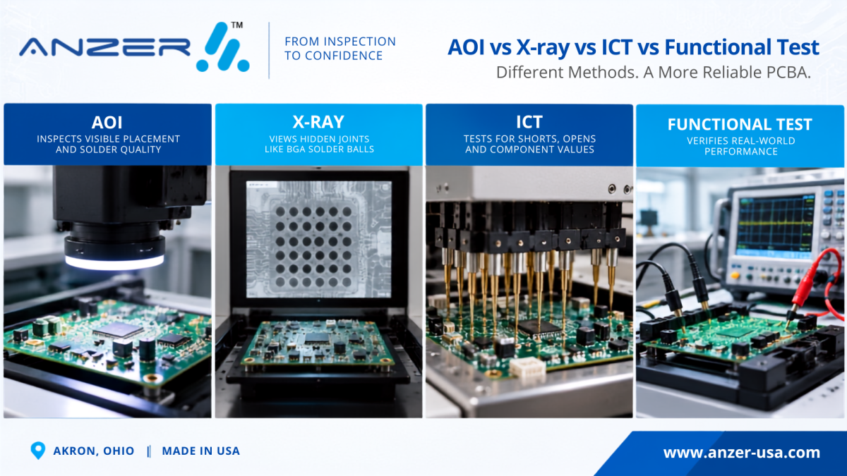
AOI, X-ray, ICT and functional testing examine different aspects of a PCBA. AOI focuses on visible assembly conditions. X-ray provides inspection of hidden solder joints. ICT checks electrical conditions such as opens, shorts and component values. Functional testing goes one step further by operating the assembly and checking whether it performs according to the defined requirements.
No single method proves everything.
For an OEM, the better approach is to match the testing strategy to the board design, components, application risk, production requirements and failure modes that matter most.
AOI vs X-ray vs ICT vs Functional Testing at a Glance
| Method | Primary purpose | What it can detect | Main limitation |
|---|---|---|---|
| AOI | Visual inspection | Component placement, visible solder defects, polarity and assembly issues | Cannot directly inspect hidden solder joints |
| X-ray | Hidden-joint inspection | Hidden solder connections, including joints beneath suitable packages | Does not prove overall functional operation |
| ICT | Electrical verification | Opens, shorts and component values | Requires appropriate test access and test strategy |
| Functional Testing | Operating verification | Behavior and performance under defined operating conditions | A failure may not identify the physical root cause by itself |
The key point is simple:
AOI asks, “Does the assembly look correctly built?”
X-ray asks, “What is happening where I cannot see the solder joint directly?”
ICT asks, “Are the electrical connections and component conditions correct?”
Functional testing asks, “Does the assembled product perform as intended?”
That distinction matters when specifying an EMS partner.
What Is AOI in PCB Assembly?
Automated Optical Inspection, or AOI, uses automated vision-based inspection to examine the assembled PCB.
AOI is particularly useful for identifying visible assembly conditions such as component placement and solder-related defects.
Depending on the programmed inspection criteria, AOI can help identify issues such as:
- Missing components
- Misplaced components
- Incorrect orientation or polarity
- Solder bridges
- Skewed components
- Other visible solder or placement anomalies
AOI is valuable because it provides an automated inspection checkpoint during PCB assembly.
However, AOI has a fundamental limitation: it is an optical inspection method.
If an important solder connection is hidden underneath a component package, the camera cannot simply look through the component to inspect the joint.
That is where X-ray inspection becomes useful.
ANZER provides AOI as part of its PCB assembly quality process.
What Is X-ray Inspection in PCB Assembly?
X-ray inspection allows manufacturers to evaluate solder connections and structures that cannot be adequately inspected from the board surface.
This is particularly relevant when a PCBA contains components with hidden solder connections, such as BGA-type packages.
X-ray inspection can provide visibility into areas that conventional optical inspection cannot directly see.
This makes it complementary to AOI rather than a replacement for AOI.
For example, a board may pass AOI because its visible components and solder features appear acceptable, while a hidden solder connection still requires further examination.
When should an OEM consider X-ray?
Consider X-ray as part of the test strategy when the design includes:
- Hidden solder joints
- BGA packages
- Dense or complex assemblies
- Reliability-sensitive assemblies
- Applications where hidden-joint defects carry significant consequences
The exact inspection requirement should be determined from the product design, customer requirements and applicable acceptance criteria.
IPC identifies IPC-A-610J as the current revision of its Acceptability of Electronic Assemblies standard, while also noting that IPC-A-610 is focused on visual quality acceptance and does not itself provide the criteria for X-ray inspection.
What Is ICT in PCB Assembly?
In-Circuit Testing, or ICT, checks electrical conditions on an assembled circuit board.
ANZER identifies ICT as a testing capability for checking:
- Shorts
- Opens
- Component values
- Electrical conditions within the assembled board
ICT therefore answers a different question from AOI.
AOI can identify a component that appears incorrectly positioned. ICT can help determine whether electrical connections and component characteristics meet the defined test requirements.
For production programs, this distinction can be important.
A board can look correct and still have an electrical problem.
ICT depends on design-for-test planning
One of the most important buyer considerations is test access.
The PCB must provide suitable access for the intended electrical test strategy. Test-point planning should therefore be considered during engineering and DFM/DFT review rather than after the PCB has already been released.
This is one reason DFM and testing strategy should be discussed together.
ANZER provides Design for Manufacturability (DFM) and Design for Assembly (DFA) support as part of its engineering capabilities.
What Is Functional Testing?
Functional testing verifies that the assembled electronics operate according to the defined functional requirements.
This is fundamentally different from simply looking at the board or checking individual electrical conditions.
Functional testing can be designed around the actual application and may verify the behavior expected from the completed assembly.
For an OEM, the question changes from:
“Was this board assembled correctly?”
to:
“Does this board actually perform the function it was designed to perform?”
That distinction is especially important for assemblies that interact with sensors, interfaces, controls, communication systems, firmware or other product-level functions.
ANZER lists functional testing as an in-house testing capability and describes it as simulating real operating conditions.
Functional Testing vs ICT: What Is the Difference?
This is one of the most common areas of confusion.
ICT is primarily an electrical verification method. Functional testing is an operating-behavior verification method.
Think about them this way:
| Question | ICT | Functional Test |
|---|---|---|
| Are there opens? | ✓ | May detect indirectly |
| Are there shorts? | ✓ | May detect indirectly |
| Are component values correct? | ✓ | May detect indirectly |
| Does the board power correctly? | Depending on test design | ✓ |
| Does the product perform its intended function? | Not the primary purpose | ✓ |
| Does the complete test sequence behave correctly? | Not the primary purpose | ✓ |
A functional test can tell you that a board does not behave correctly.
ICT can often provide more specific electrical information that helps isolate the underlying assembly problem.
They solve different problems.
AOI vs X-ray: Why Both Can Matter
AOI and X-ray are also complementary.
AOI is well suited to visible assembly inspection.
X-ray becomes valuable when important features are hidden from direct optical inspection.
A simplified example:
AOI:
Component placement → visible solder → polarity → visible assembly defects
X-ray:
Hidden solder joint → internal connection → hidden solder condition
The decision should therefore not be:
“Should I choose AOI or X-ray?”
It should be:
“Which physical features of this PCBA require which type of inspection?”
Can a PCBA Pass AOI and Still Need Functional Testing?
Yes.
Passing AOI does not mean that a PCBA has demonstrated complete functional operation.
AOI primarily examines visible assembly conditions. Functional testing examines defined operating behavior.
The two tests therefore provide different evidence.
A board can have acceptable-looking component placement and solder conditions while still having an electrical, configuration or functional issue that only becomes apparent when the board is powered and operated.
That is why an OEM should avoid treating “AOI passed” as equivalent to “product validated.”
Can a PCBA Pass X-ray and Still Fail Functional Testing?
Yes.
X-ray inspection and functional testing answer different questions.
X-ray can provide valuable information about hidden physical connections.
It does not, by itself, demonstrate that the complete electronic assembly performs every required function.
For example, a board can have acceptable hidden solder connections but still fail because of an issue outside the specific physical condition being examined by X-ray.
Inspection evidence and functional evidence are not interchangeable.
Which PCB Test Method Is Best?
There is no universally “best” test.
The better question is:
Which test method provides evidence against the failure modes that matter for this product?
Your test strategy should consider:
- Board complexity
- Component package types
- Hidden solder connections
- Required test access
- Production volume
- Application risk
- Customer specifications
- IPC workmanship requirements
- Functional requirements
- Documentation and traceability requirements
For a simple assembly, extensive testing may not be justified.
For a complex or high-reliability assembly, relying on a single inspection method may leave important failure modes unaddressed.
Testing Should Start During PCB Design
One of the most common manufacturing mistakes is treating testing as something that happens after PCB design is complete.
Test strategy should be considered earlier.
During DFM/DFT review, engineering teams should ask:
- Where will electrical test access be located?
- Which nets need to be tested?
- Which components require special inspection?
- Are there hidden solder connections?
- What functions need to be verified?
- What pass/fail limits will be used?
- What test documentation will the manufacturer need?
- What defects are most important to catch before shipment?
This is where Design for Manufacturability and Design for Test become practical manufacturing considerations rather than separate engineering exercises.
For OEMs developing a new board, ANZER’s electronic design for manufacturability service is a relevant starting point.
How the Methods Can Work Together
A practical PCBA quality strategy can use several inspection and test layers.
A simplified example is:
PCB Assembly
↓
AOI
↓
X-ray where applicable
↓
ICT where applicable
↓
Functional Testing
↓
Final Inspection / Documentation
This is not a mandatory sequence for every product.
The appropriate process depends on the board, customer requirements, production environment and test plan.
ANZER’s verified PCB assembly process includes AOI, X-ray where applicable, ICT and functional testing, followed by additional assembly and finishing steps when specified.
What OEM Buyers Should Ask an EMS Provider
When comparing PCB assembly suppliers, don’t simply ask:
“Do you offer testing?”
Ask more specific questions.
Inspection
- Do you perform AOI?
- When is AOI performed?
- How are inspection results handled?
- Can you inspect hidden solder joints with X-ray?
Electrical testing
- Do you offer ICT?
- What test access does the PCB require?
- Can test requirements be reviewed during DFM?
- Is flying probe available when appropriate?
Functional testing
- Can the manufacturer execute the customer’s functional test procedure?
- What equipment or fixtures are required?
- What are the documented pass/fail criteria?
- How are failures recorded and investigated?
Quality and compliance
- What workmanship standard applies?
- Is the build Class 2 or Class 3?
- What documentation is retained?
- What traceability requirements apply?
- Does the manufacturing partner understand the requirements of the end application?
For regulated applications, these questions become even more important.
ANZER manufactures to IPC Class 2 and Class 3 requirements and holds ISO 9001:2015, ISO 13485:2016 and AS9100D certifications.
Why DFM and Testing Belong in the Same Conversation
A test strategy can expose problems, but good manufacturing engineering should also work to make those problems easier to detect.
DFM review can identify manufacturing risks before production.
DFT planning can improve access to the electrical conditions that need to be verified.
Together, they can help engineering teams move from:
“Can we manufacture this PCB?”
to:
“Can we manufacture, inspect, test and document this PCB consistently?”
That is a much more useful question for an OEM production program.
ANZER’s Approach to PCBA Testing
ANZER provides PCB assembly from prototype through production and lists AOI, X-ray inspection, ICT, flying probe, functional testing and burn-in testing among its manufacturing and test capabilities.
The company also supports DFM, DFA, BOM optimization and testing strategy consultation during the engineering phase.
For buyers in regulated or high-reliability markets, ANZER’s quality framework includes IPC Class 2 and Class 3 manufacturing, ISO 13485:2016 for medical manufacturing and AS9100D for aerospace manufacturing.
The practical objective is not to add tests simply because more testing sounds better.
It is to build a test strategy that gives the OEM meaningful evidence at the right stages of manufacturing.
Conclusion
Functional testing vs ICT vs AOI vs X-ray is not really a competition between four technologies.
Each method answers a different manufacturing question.
- AOI checks visible assembly conditions.
- X-ray helps inspect hidden solder connections.
- ICT verifies defined electrical conditions.
- Functional testing verifies that the assembly performs its intended functions.
The strongest PCBA test strategy matches these methods to the actual design and risk profile of the product.
For OEMs, the conversation should start during engineering, not after the first production board fails.
If you are preparing a PCB assembly RFQ, include the PCB files, BOM, assembly drawings, test requirements, applicable workmanship class, functional test procedure and any traceability or documentation requirements available at the time of quotation.
ANZER can review the manufacturing and testing requirements as part of the PCB assembly process.
For a production discussion, use ANZER’s Get a Quote page.
FAQs
Is AOI the same as functional testing?
No. AOI is primarily a visual inspection method for assembly conditions. Functional testing verifies whether the assembled electronics perform defined functions.
Is X-ray better than AOI?
Neither is universally better. X-ray is useful for hidden features that optical inspection cannot directly see, while AOI is well suited to visible component placement and solder conditions.
What does ICT test on a PCB?
ICT can check defined electrical conditions such as shorts, opens and component values. The exact coverage depends on the board design and test strategy.
Does every PCB assembly need AOI, X-ray, ICT and functional testing?
No. The appropriate combination depends on the PCB design, component packages, production requirements, application risk and customer test requirements.
When should PCB testing be planned?
Testing should be considered during PCB design and DFM/DFT review. Test access, required measurements, hidden joints and functional requirements should be identified before production whenever possible.